MIL-C-60898/4(MU)
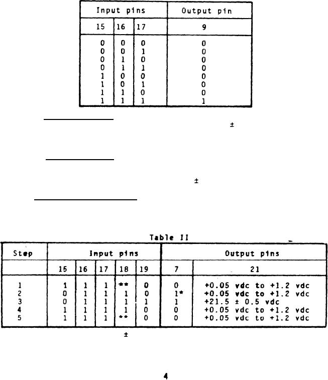
Table I
3.4.2.2 Output pin 23.
With a logic input "1" applied to
0.5 vdc.
pin 19, the voltage at pin 23 shall be +18.4
With
a logic input "O" applied to pin 19, the voltage at pin 23
shall be greater than +0.01 vdc but less than +1.2 vdc.
3.4.2.3 Output pin 6. The voltage between pin 6 (+) and pin
28 shall be greater than +0.01 vdc but less than +1.2 vdc for
the conditions of 3.4.1.
With pin 13 grounded, the voltage be-
tween pin 6 and pin 28 shall be +21.5
0.5 vdc.
3.4.3 Sequence and timing.
With the inputs applied in the
sequence specified in Table II, there shall be the outputs
specified in Table II at pin 7 and at pin 21.
* Logic "1" delayed 500
25 milliseconds from the time
pin 15 becomes a logic "O".
** Apply a "O" for 1 to 5 seconds and then apply a "1".
For Parts Inquires call Parts Hangar, Inc (727) 493-0744
© Copyright 2015 Integrated Publishing, Inc.
A Service Disabled Veteran Owned Small Business